Good adhesion is important in many steps of electronic manufacturing. One of the most critical steps is the application of the photoresist. Proper photoresist adhesion is of utmost importance for the successful lithographic process. Loss of adhesion in the development or etching process will result in patterning errors that are detrimental to the device being manufactured. The need for the adhesion promoter between the photoresist and the silicon wafer has been long recognized. One of the most commonly used priming methods is hexamethyldisilazane (HMDS) treatment.
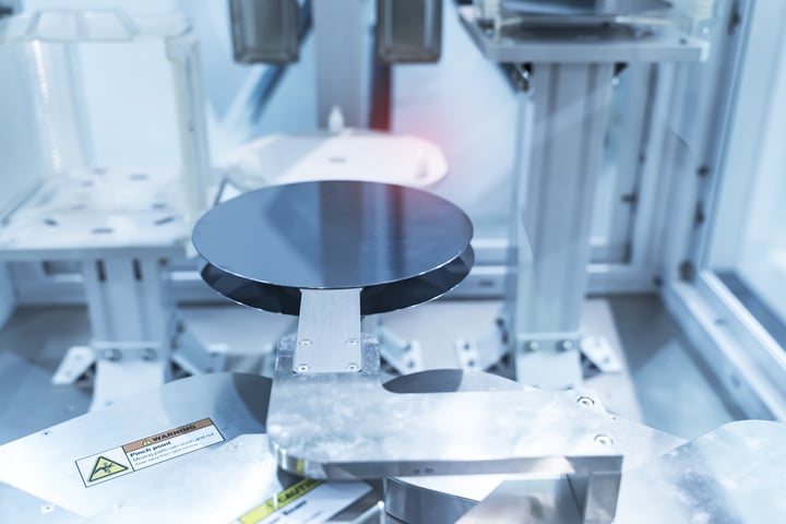
Hexamethyldisilazane (HMDS) priming is commonly used before the application of the photoresist. The utilization of the HMDS as a photoresist adhesion promoter was described for the first time in U.S. Patent 3,549,368 by R.H. Collins and F.T. Devers of IBM in 1970. The process has evolved from a solution-based method where wafers were dipped into an HMDS solution to a vapor-based process. Although HMDS can be applied on the wafer by spin coating, this is not typically recommended as vapor evaporation from the thick layer of HMDS can cause problems at a later stage. Most typically HMDS is applied in a vacuum chamber that combines the heating of the substrate with the exposure to the HMDS vapor.
HMDS improves the adhesion of the photoresist
The surface of the silicon wafer is typically hydrophilic due to adsorbed layer of water from the ambient humidity. For proper adhesion of the photoresist, the surface needs to be rendered more hydrophobic to match better with the chemistry of the photoresist. The first step in the process is called a dehydration bake. As the name proposes, the purpose of the step is the removal of the water from the wafer surface. This step is often performed in a vacuum and requires a temperature of around 140 to 160 °C. If the water layer is not removed, there is a risk of delamination of the photoresist during subsequent development or chemical etching processes. However, after this step, the surface of the wafer is still hydrophilic as dehydration leaves the surface to its native state. In the native state, the silicon wafer has a thin layer of native oxide on top that forms when exposed to atmospheric humidity. Chemically this is seen as OH groups at the silicon surface. For photoresist to adhere properly, the surface needs to be more hydrophobic (water-repellent).
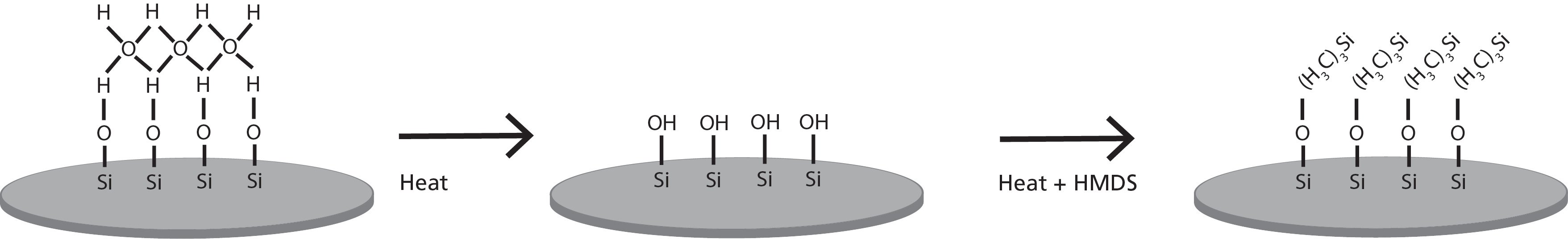
Whereas the dehydration bake removes the excess material (i.e. the adsorbed water) from the wafer surface, the HMDS treatment will add a monolayer of material to make it more attractive to the photoresist. After a dehydration bake, the surface is exposed to vapor HMDS, typically in a hot priming oven set to 130 to 160 °C. The OH groups on the wafer surface will react with the methyl groups of HMDS which will make the surface more hydrophobic. The surface is then better matched with the chemistry of the photoresist but will also be less prone to water absorption.
As photoresist adhesion is such a critical part of the lithography process, it is important to ensure that the HMDS treatment has been successful. This can be easily done with the water contact angle measurements. As the surface of the silicon wafer before the HMDS treatment is hydrophilic, the water contact angle is relatively low, around 40°. After the HMDS treatment, the water contact angle increases significantly due to the more hydrophobic nature of the treated surface. Optimum results are typically achieved with contact angles between 65° and 80°.
Water contact angle measurements are easy to perform as only a small drop of deionized water is needed for the measurements. The water contact angle is extremely surface sensitive and can detect small variations between the different samples and across the surface. If you would like to know more about how contact angle measurements can be used to predict adhesion, please download the white paper below.


Susanna is an Application Scientist at Biolin Scientific. In her PhD thesis, she developed fabrication methods for a new type of inorganic-organic polymers. Microfabricated polymer chips were utilized as tool for biomolecule separation in analytical chemistry.