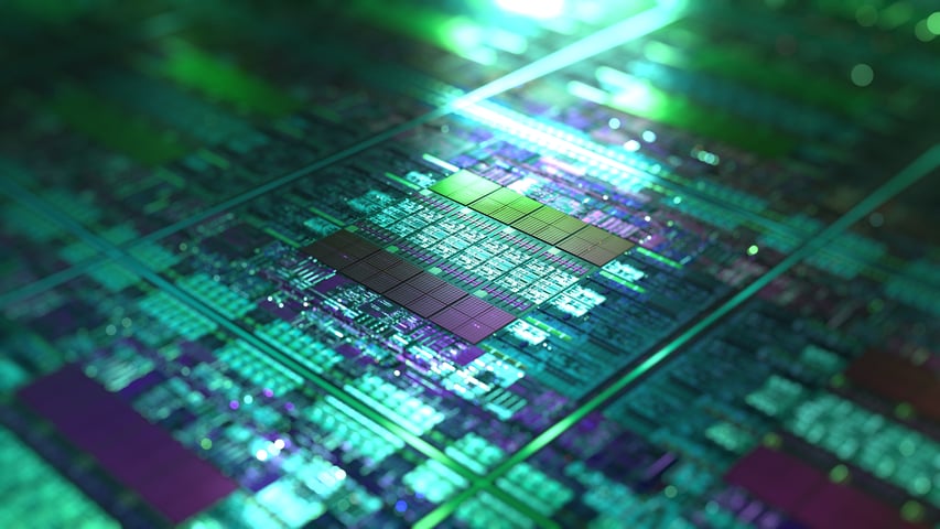
In electronics manufacturing, whether it is on a wafer level or in PCBs, there are multiple materials involved that need to adhere to each other either permanently or for the duration of a process step. Independent on which type of adhesion process you are dealing with; adhesion needs to be reliable and successful every single time.
One of the most critical requirements for good adhesion is surface cleanliness.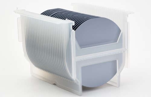 RCA cleaning is the standard cleaning method for silicon wafers before processing. The purpose of the cleaning is to remove all foreign material from the surface including dust, oil, silicon dust, etc. The cleaning steps are divided into two; RCA1 and RCA2. RCA1 will remove any organic contamination whereas RCA2 takes care of the ionic and metallic contamination. Dilute hydrogen fluoride solution is often used in between to remove the thin oxide layer. Water break tests are commonly used to check the status of the surface after the cleaning procedure. Water contact angle measurements offer a traceable and quantitative way to do the same.
Proper photoresist adhesion is of utmost importance for the successful lithographic process. 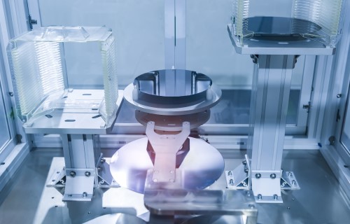 Loss of adhesion in the development or etching process will result in patterning errors that are fatal for the device being manufactured. The need for the adhesion promoter between the photoresist and the silicon wafer has been long recognized.
Hexamethyldisilazane (HMDS) priming is commonly used before the application of the photoresist. The water contact angle on a silicon wafer is typically quite low due to adsorbed surface layer of water from ambient humidity. If the water layer is not removed before the photoresist application, there is a risk of complete delamination of the photoresist during subsequent development or chemical etching processes. After a dehydration bake, a hydrophobic HMDS coating is often applied to render the surface more hydrophobic and thus less prone to water absorption. Water contact angle measurements can be used to find the optimum HMDS treatment protocol as well as to check that the treatment has been successful.
Removal of the excess flux is an important part of the soldering process. 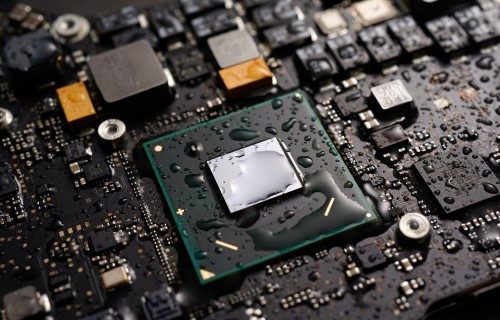 This is because some fluxes are corrosive, and their residues may continue their activity and harm the circuit boards at a later stage. Due to the detrimental effects of flux on the PCBs, there is a vast range of cleanliness tests available for PCBs. These include ion chromatography, resistivity of solvent extract (ROSE) testing, surface insulation resistance testing (SIR), and visual tests. Out of those ROSE is by far the most popular one. The main advantage of the ROSE test is the speed of testing together with the low price. The problem is that it is not able to detect all kinds of contamination, and those that it does are averaged over the whole surface tested. Water contact angle measurements offer a great alternative for the ROSE test. Water contact angle measurements are performed by placing a drop of water on the PCB. If the water beads up (i.e., the contact angle is high), the surface is not ready for conformal coating. If the water spreads (i.e., the contact angle is low) the surface is free of organic contaminants, and the coating can be done. One advantage of a contact angle measurement is that it can be done also on extremely small areas.
Conformal coatings are used to protect the PCBs from environmental conditions such as high humidity, a range of airborne contaminants, and varying temperatures.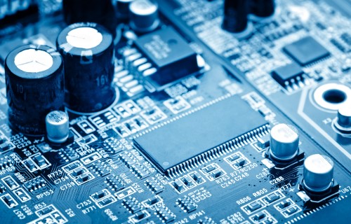 Most of the carrier materials for PCBs are made of glass fiber reinforced plastics which typically have low surface free energy values at around 40 to 45 mN/m. Furthermore, the surface free energies of the individual components and assemblies vary greatly. This makes the conformal coating difficult and adding a cleaning step might not be sufficient to increase the surface free energy to the required level. As a common rule, the surface tension of the conformal coating should be at least 10 mN/m lower than the surface free energy of the substrate. Plasma activation of the PCBs can be used to increase the surface free energy and thus ensure more homogenous wetting of the PCB. Contact angle measurements can be used at various stages of the process. First to check the surface wettability at the beginning and then to find proper plasma treatment parameters to reach the required levels. Contact angle also provides an excellent tool for quality control purposes to make sure that the process is under control at all times.

Susanna is an Application Scientist at Biolin Scientific. In her PhD thesis, she developed fabrication methods for a new type of inorganic-organic polymers. Microfabricated polymer chips were utilized as tool for biomolecule separation in analytical chemistry.